This project came up in order to experiment with op amps and test some ideas and concepts.
The project is build around an opamp from Microchip, the MCP660 [1]. This is a package with three 60 MHz opamps.
The PCB is designed with KiCAD [2].
The idea is to get an input signal into the analog front end, use a voltage divider to lower the voltage and then use the op amp to amplify it in order for example to match the full dynamic range of an ADC. The whole front end should be able to be controled digitally by for example a microprocessor (MCU).

Looking at the schematic:

The first part is a relay, which is able to switch between AC and DC. For AC a 100nF capacitor can be placed in the signal path. Depending on the frequency this one might be replaced by a bigger capacitor.
The relay is controlled depending if HIGH or LOW, which way to choose. In order to not put too much load on the digital pin controlling the relay a transistor is used for amplification. Since the relay is an inductor, which loads when switching, a diode is placed to protect against returning currents.
The voltage divider
After the AC/DC selection the signal is passed into a voltage divider. The divider breaks down the input voltage to a fraction of it, small enough to not overload the system. But also to provide a high input impedance to the input port of the front end. A protection diode is placed after the voltage divider to make sure that no too high voltages are destroying the following op amp.
The capacitive voltage divider, which is placed in parallel with the restive one, is there in order to compensate for the capacitance introduced by the components like diode, traces and the resistors. Without the capacitive voltage divider the whole chain acts like a low pass filter limiting the bandwidth. The capacitive voltage divider compensates for that and should be designed according to how much capacitance is in the front end.
The layout contains a DAC_Offset pin, which can be connected to a DAC or ground. With this pin an offset voltage can be introduced lifting the input signal in order to run in in the positive range of the opamp. The signal part being below GND are clipped.
In order to not introduce more disturbing parts, the signal is buffered by a voltage follower (analog buffer). This is nice since it decouples the rest of the circuit from the input stage. After the analog buffer, the signal is fit into the opamp which is used to amplify the signal and match it to the dynamic range of the possible following ADC, or whatever is connected to the output connector.
The opamp is run in non-inverting mode. The idea was to build a kind of variable gain amplifier (described in the next section). This is achieved by having different resistors switchable connected.
Which resistor is connected to the circuit is controlled by a 74HC595 shift register.
After the variable gain amplifier one more protection diode comes in order to protect the following circuitry for over-voltage.
The variable gain amplifier
In order to be able to change the gain of the opamp the voltage divider between output,inverting-input(“-“) and ground has to be variated.
Since it is hard to change the resistor between output and inverting-input, the resistors between inverting-input and ground were made switchable. This is achieved by introducing a SI2302 MOSFET between them. The MOSFET is a special N-channel FET having a very low “Drain-Source On-Resistance” in order not too add additional resistance to the voltage divider.
One very important issue if constructing like this is, that the opamp can only be run with signals above ground (>=0 V). With negative signals the FET does not work as expected, since it is not a simple switch and behaves differently depending on the polarity.
The system works in the following way: If the FET is in “ON” stage it connects the resistor to ground and we have a voltage divider in the way: V—-R—-R—-GND, in “OFF” stage we have V—-R—-R–\ -GND a broken connection. In this way one can switch a single or a combination of resistors ON and OFF and with this change the amplification.
There are at least two issues with this construction:
-The first one was aleady said is that one has to operate with positive voltages only.
-The second is that one is introducing the more switchable stages and FETs one adds more and more capacitance into the system. This has bad effects on the bandwidth of the amplifier.
This can be seen in the following measurements:
 |
 |
 |
 |
It can be seen that if sending into the system a 1 MHz square wave or sine wave one can see disturbances. This is coming from the capacitance of the FETs and traces. One way to do some compensation is to solder a resistor between the Inverting- and Non-Inverting-input. This does do some compensation but on the cost of reducing the bandwidth.
Therefor such a design only works for low frequency applications. One workaround can be replace the FETs by analog switches, having less capacitance and which will also solve the problem of being limited to positive voltages. But they have a higher price compared to the FETs.
Otherwise there exist ICs which contain the whole construction already in one signal chip and which are optimized for high bandwidth applications.
The system itself works for low frequencies this can be seen in the gain measurements, where the output was measured under different amplification stages. It should be kept in mind that the more amplification the amp gives the lower is the bandwidth of the opamp.
 |
 |
 |
 |
The amplification for the non-inverting opamp is given by
A=1+200 Ohm/X
where X is the set resistance.
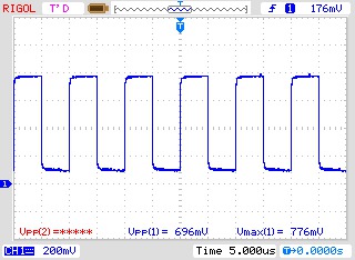
For an input of ~352mV @ 200 kHz the above measurements were taken:
1M ohm : A~=1: Vout=380mV

200 ohm : A=2: Vout=696mV

50 Ohm : A=5: Vout=1.72V

22 Ohm : A=10.1: Vout = 3.36V
which fits pretty good with the equation above.
Controlling the analog front end by a microprocessor
In order to switch between AC/DC and the different amplification stage a shift register is used holding the settings. The shift register can be controlled by three wires (Two clock signals and a data line). The shift register is connected to a MCU in this example and Arduino and the bits are set as needed.
A simple example code is listed in the following:
//Control a 74HC595 IC

const int SER=7; //pin of the serial data line
const int SRCLK=5; //pin of the serial clock
const int RCLK=6; //pin of the clock whcih shifts the serial register into the data register

char incomingByte;
char Data[10];
int index;
String myString="";

// the setup routine runs once when you press reset:
void setup() {
  // initialize serial communication at 9600 bits per second:
  Serial.begin(9600);

  pinMode(SER, OUTPUT);
  pinMode(SRCLK, OUTPUT);
  pinMode(RCLK, OUTPUT);

  digitalWrite(SER,LOW);
  digitalWrite(SRCLK,LOW);
  digitalWrite(RCLK,LOW);
}

/*This function shifts in the input byte into the shift register
*/
void shiftIn(byte InByte){
  Serial.print("Shift In: ");
   //shift into the serial register

  for(int i=0;i<8;i++){

/*    if(InByte & 1<<i){
      digitalWrite(SER,HIGH);
      Serial.print("1");
    }
    else{
      digitalWrite(SER,LOW);
      Serial.print("0");
    }*/
    digitalWrite(SER,InByte & 1<<7-i);
    digitalWrite(SRCLK,HIGH);
    delay(10);
    digitalWrite(SRCLK,LOW);
    delay(10);
  }
  //copy serial into data register
  digitalWrite(RCLK,HIGH);
  delay(10);
  digitalWrite(RCLK,LOW);
  delay(10);
  Serial.println(" done");
}

/* This function converts a string of eight '1' and '0' into a byte
  It returns -1 if an error occures adn 0 if no error
*/
int convertStringToByte(String ByteString, byte &OutByte){
  Serial.println(ByteString.length());
  Serial.println(ByteString);
  if(ByteString.length()!=8){
    Serial.println("String != 8");
    return -1;
  }

  OutByte=0;
  for(int i=0;i<8;i++){
    if(ByteString[i]=='1')OutByte=OutByte | 1<<7-i;
    else if(ByteString[i]=='0')OutByte=OutByte;
    else{
       Serial.println("String contains wrong character");
       return -1;
    }
  }
  return 0;
}

// the loop routine runs over and over again forever:
void loop() {


    while (Serial.available() > 0) {

      // read the incoming byte:
      incomingByte = Serial.read();
      Serial.println(incomingByte);
      if(incomingByte=='\n'){
        myString=String(Data);
        myString=myString.substring(0, myString.length()-1);
        Serial.println(myString);
        byte OutByte;
        if(convertStringToByte(myString,OutByte)==0){
          shiftIn(OutByte);
          //shiftIn(OutByte);//Write twice when the relay turns on some bits are not correct
          Serial.println((char)OutByte);
        }
        index=0;
      }
      else{
        Data[index]=incomingByte;
        index++;
        Data[index]='\0';//Terminate the char array
      }


  }

}
To conclude this project shows clearly the difficulties with analog designs. It works fine for low frequency applications but is limited for higher frequencies.
[1] http://www.microchip.com/MCP660
[2] http://kicad-pcb.org/
The code for the Arduino and the KiCAD design can be found on GitHub:
https://github.com/digibird1/VariableGainAmplifier
It can be checked out with:
git clone https://github.com/digibird1/VariableGainAmplifier
